

Development History
-
2023
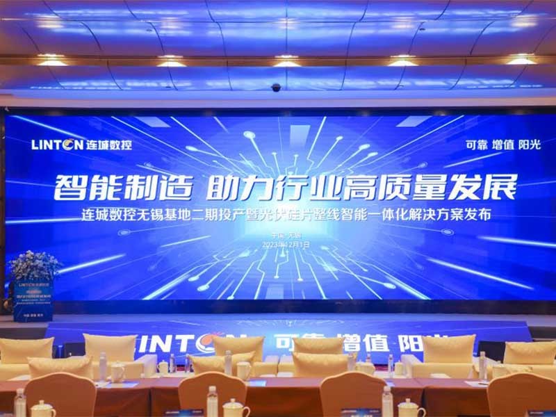
On December 1, Linton CNC held the second phase of Wuxi base put into production and the release of PV wafer whole line intelligent integrated solution.
-
2023
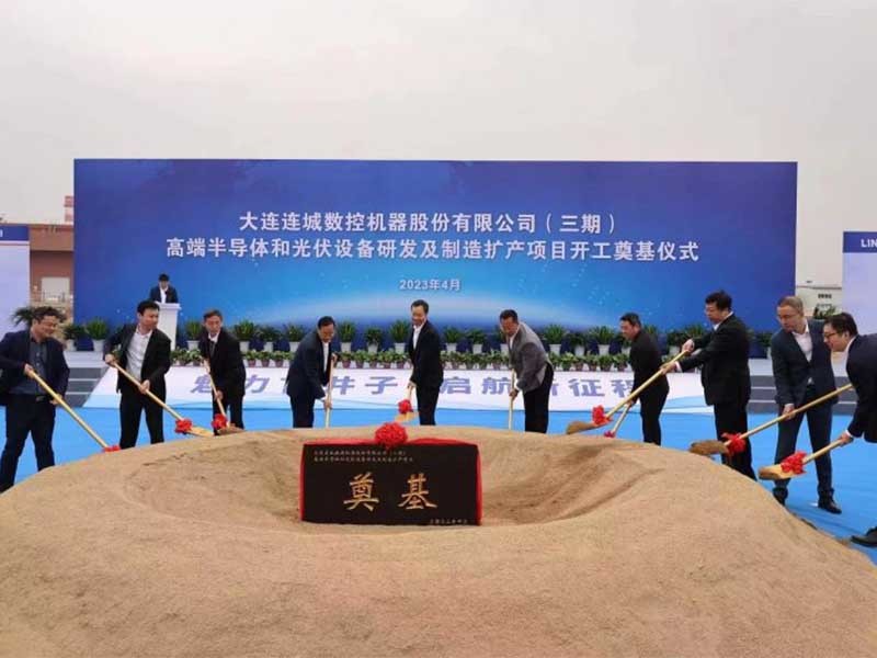
In April, Linton CNC Dalian Base Phase III Project held a groundbreaking ceremony.
-
2023
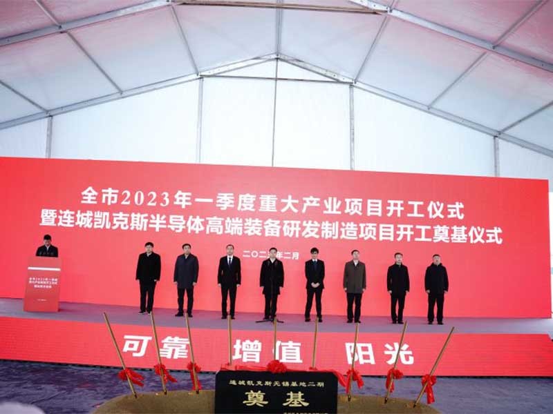
In February, Linton CNC Wuxi Base Phase II held a groundbreaking ceremony.
-
2021
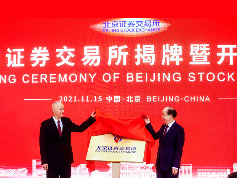
On November 15, Linton CNC became the first batch of enterprises listed on the Beijing Stock Exchange.
-
2021
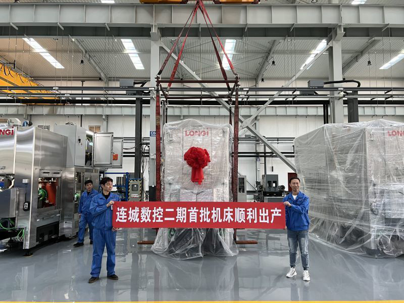
In October, the first silicon carbide synthesis furnace and crystal growing furnace of Linton CNC were successfully launched. The second phase of Dalian plant was put into operation.
-
2021
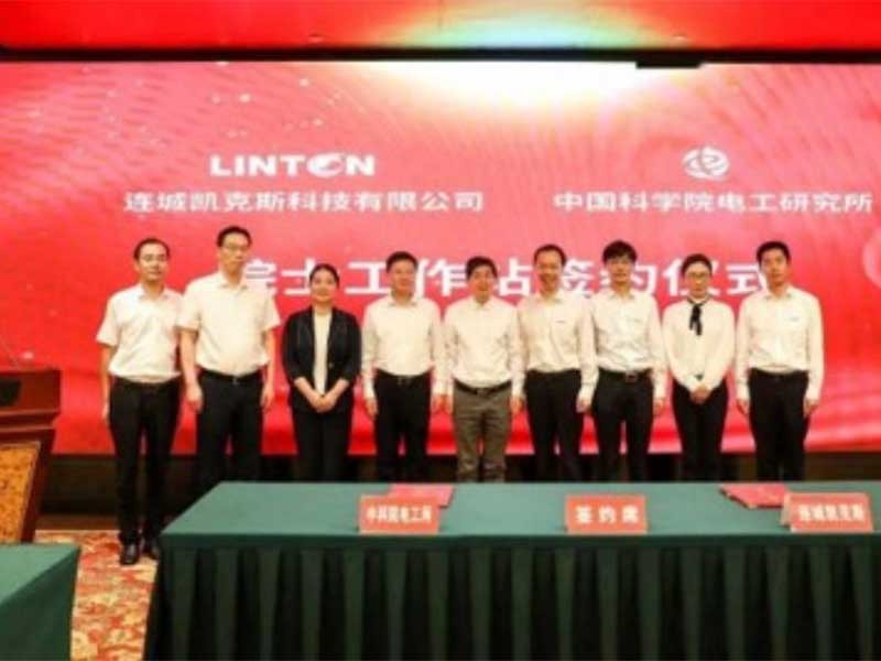
In September, Linton Kayex and the Chinese Academy of Sciences Institute of Electrical Engineering jointly set up an academician workstation for IC-level single crystal furnace superconducting magnetic field research and development.
-
2021
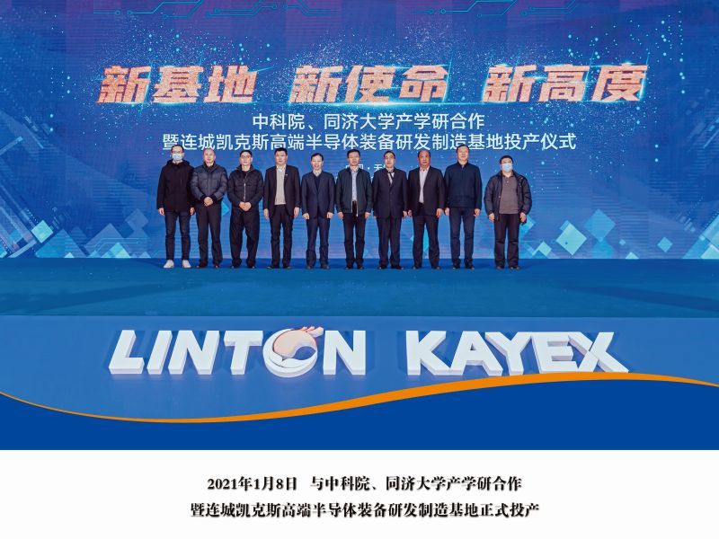
On January 8, Linton Kayex high-end semiconductor equipment R & D and manufacturing base officially put into production.
-
2020
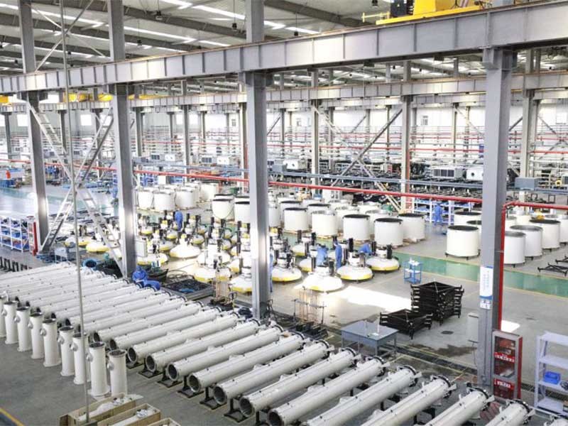
In November, Linton Kayex Technology Co., Ltd. officially completed the relocation of the new base.
-
2020
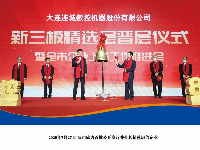
On July 27th, Dalian Linton CNC Machinery Co., Ltd. held the "Selected Layer Promotion and Stock Public Offering Ceremony", officially ringing the bell to open the market, and became the first enterprise in the Northeast region to land on the Selected Layer of the New Third Board.
-
2020
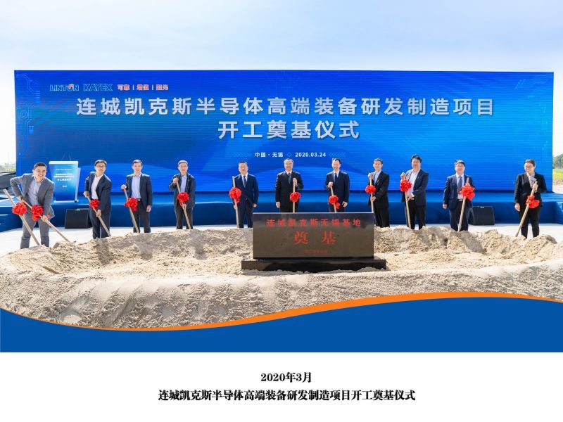
In March, Linton Kayex held the semiconductor high-end equipment R & D and manufacturing project groundbreaking ceremony.
-
2019
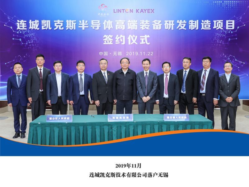
In November, Linton Kayex Technology Co., Ltd. settled in Wuxi.
-
2019
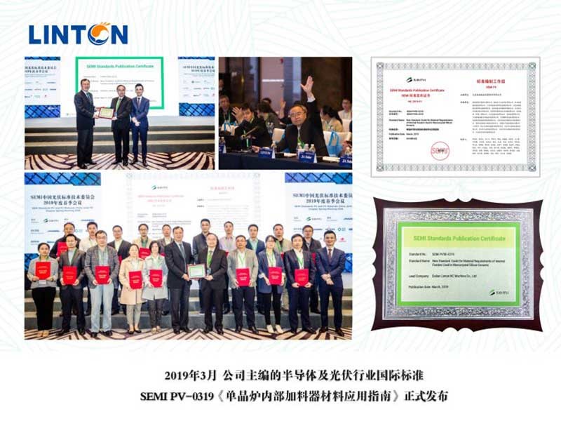
In March, SEMI PV-0319, the international standard for semiconductor and photovoltaic industry, "Application Guide for Materials of Internal Feeder of Single Crystal Furnace", edited by the company, was officially released;
-
2019
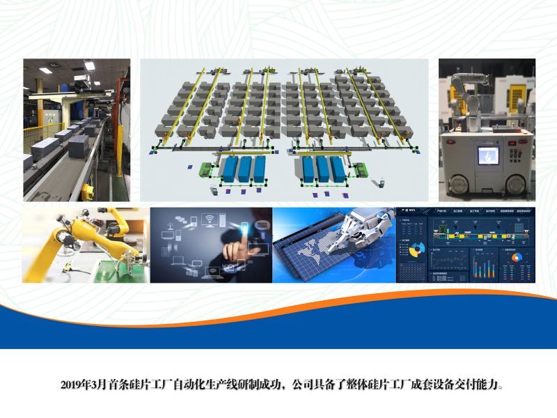
In March, the first wafer factory automated production line was successfully developed, and the company has the ability to deliver complete sets of equipment for the whole wafer factory.
-
2018
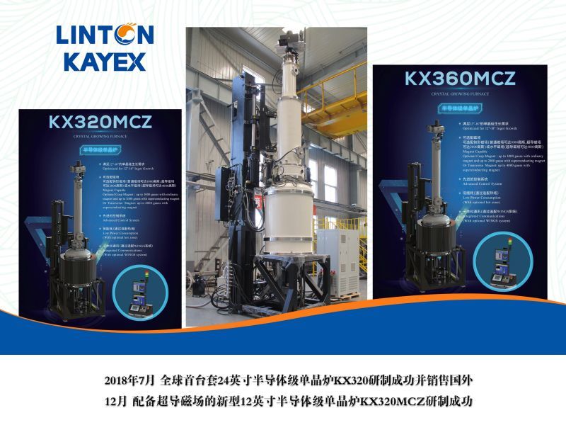
In July, the world's first 24 inch semiconductor crystal furnace KX320 was successfully developed and sold abroad; In December, the new 12 inch semiconductor grade single crystal furnace KX320MCZ with superconducting magnetic field was successfully developed;
-
2017
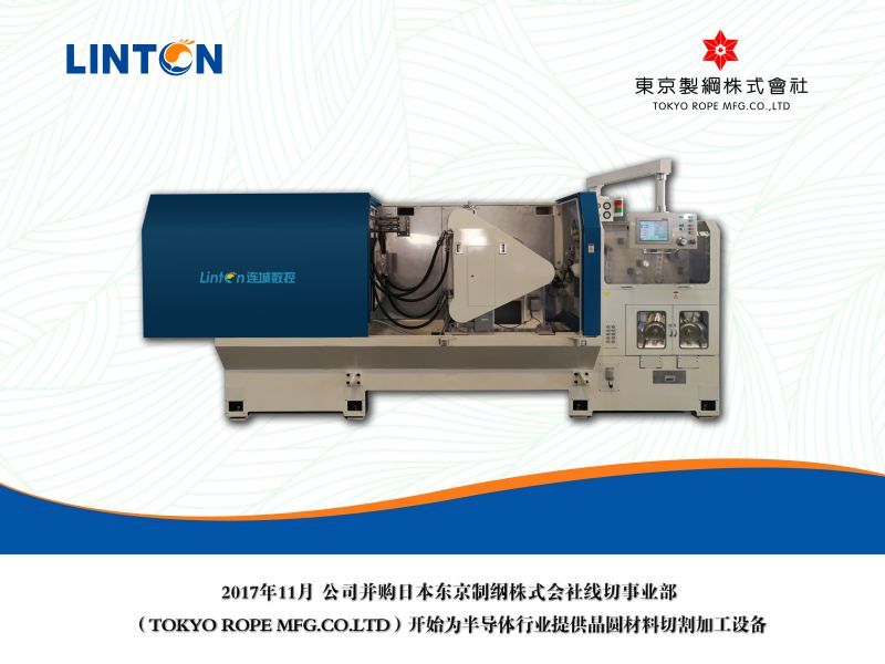
In November, the company acquired TOKYO ROPE MFG. LTD, and began to provide wafer material cutting and processing equipment for the semiconductor industry;
-
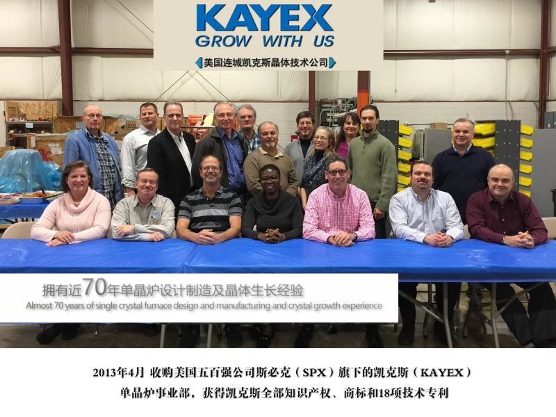
2013
In April, the company acquired KAYEX Mono Crystal Furnace Division under SPX, a top 500 company in the United States, and obtained all intellectual property rights, trademarks and 18 technical patents of the company;
-
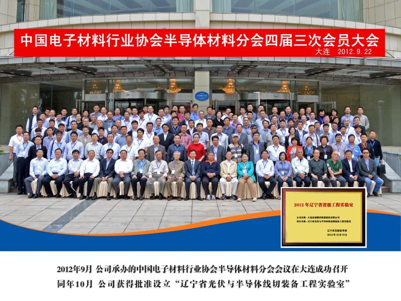
2012
In September, the company hosted the semiconductor materials branch meeting of China Electronic Materials Industry Association, which was successfully held in Dalian; in October, the company was approved to set up the "Liaoning Provincial Photovoltaic and Semiconductor Cutting Equipment Engineering Laboratory";
-
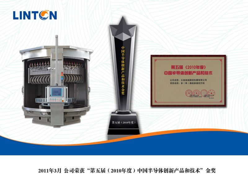
2011
In March, the company was honored with the Gold Award of "The Fifth (2010) China Semiconductor Innovative Products and Technologies"
-
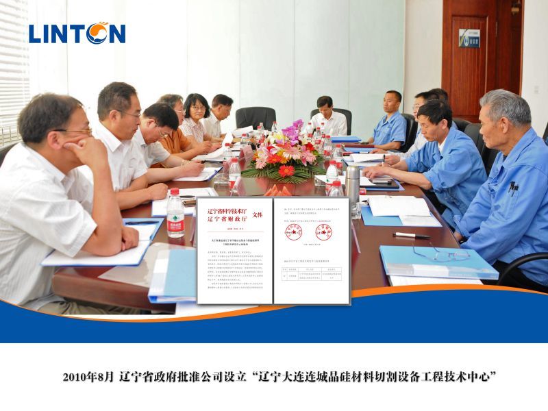
2010
In August, Liaoning Provincial Government approved the establishment of "Liaoning Dalian Linton Crystalline Silicon Material Cutting Equipment Engineering Technology Center".
-
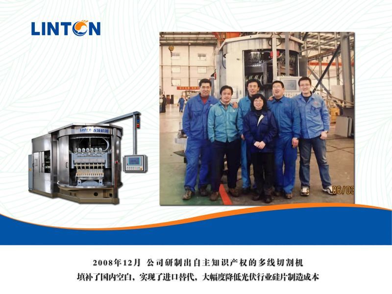
2008
In December, the company developed a multi-wire cutting machine with independent intellectual property rights, which filled the gaps in the domestic market, realized import substitution, and substantially reduced the cost of wafer manufacturing in the photovoltaic industry
-
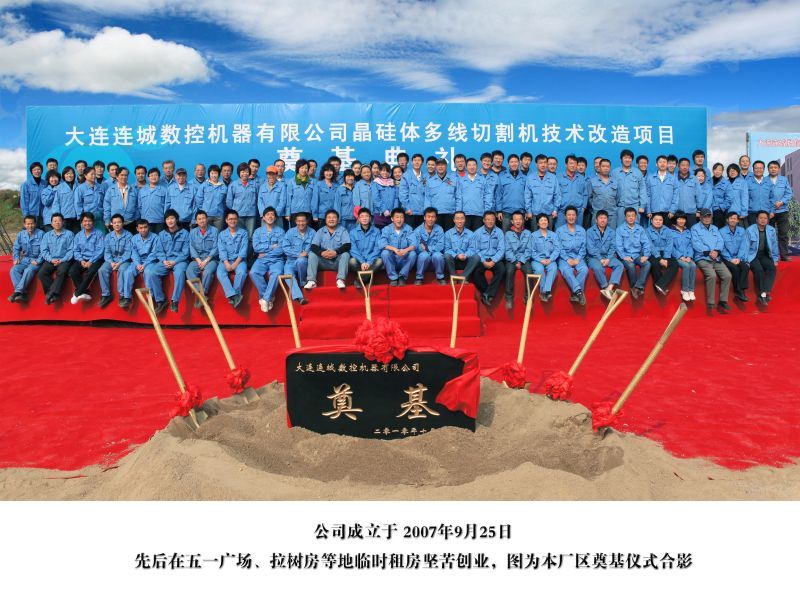
2007
On September 25, the company was established. It rented a temporary room in Wuyi Square and La Shufang and other places in different time to exert business. The following picture shows the group photo of the groundbreaking ceremony of the plant.

Dalian Base: No. 30, Huantai West Street, Yingchengzi Industrial Park, Ganjingzi District, Dalian City
Wuxi Base: No. 15 Jinghong Road, Xishan District, Wuxi, Jiangsu Province
Tel: +86-510-68088419
Stock Code
920368
Dalian Base: No. 40 Yingri Road, Ganjingzi District, Dalian, Liaoning Province
Wuxi Base: No. 15 Jinghong Road, Xishan District, Wuxi, Jiangsu Province
Tel: +86-510-68088419
Stock Code
920368
Copyright©2024 Dalian Linton NC Machine Co., Ltd.

大连连城数控机器股份有限公司
大连连城数控机器股份有限公司(简称“连城数控”) 2007年9月成立, 是一家集科研、生产、创投于一体的北交所上 市公司( 835368.BJ),下属控股公司14家,参股公司8家。公司旗下拥有5家高新技术企业,1个海外研发中心,2个省部级 研发中心,3个市级研发中心,1个院士工作站,1个校企联合研发中心;半导体及光伏行业国际标准起草单位。
公司拥有4名合作院士及-支以博士、行业专家为核心的技术研发与管理团队,累计获得国家专利300余项。
公司业务领域涉及半导体与太阳能光伏单晶硅生长及硅片切磨加工设备,太阳能光伏硅片、电池片清洗、制绒、刻蚀、 组件串焊、叠焊设备,半导体薄膜生长设备(ALD、 PECVD、 LPCVD等),蓝宝石、碳化硅等新型半导体材料晶体生长及切磨加工设备,以及硅料微波加热破碎、氩气净化回收设备。同时公司具备提供工业4.0背景下太阳能光伏智能制造、智慧工厂的解决方案及软硬件交付能力。
连城数控在光伏与半导体装备技术领域进行全产业链布局,公司致力于成为全球领先的光伏与半导体集成服务商。
连科半导体是大连连城数控机器股份有限公司的全资子公司。2007年, 大连连城数控机器股份有限公司(连城数控835368)正式成立,系国家级高新技术企业、行业标准的起草单位。公司拥有“辽宁省晶硅材料工程技术研究中心”及“辽宁省大连市光伏与半导体硅材料切割设备工程实验室”。公司秉承“可靠、增值、科学”的企业理念,倡导“反应迅速、乐于沟通、信守承诺、追求结果”的工作作风,致力于成为全球领先的半导体集成服务商。2013年 ,成立美国连城晶体技术有限公司,并购美国500强公司斯必克(SPX)旗下拥有60年历史的凯克斯(KAYEX)单晶炉事业部获得凯克斯(KAYEX)全部知识产权、商标和18项技术专利。
2021年,中科院、同济大学产学研合作项目和连科半导体高端半导体装备研发制造基地在无锡正式投产,助力连城集团 在半导体装备与技术研发方面再.上新台阶。公司研发的300毫米半导体单晶炉处于世界领先水平,拥有18项技术专利,先后推出优化改进的新型8英寸、12英寸, 并研制出24英寸半导体级单晶炉。
连科半导体有限公司是-家宽禁带半导体领域的关键设备供应商,主要从事碳化硅晶体生长炉,碳化硅粉体合成炉蓝宝石炉及碳化硅同质外延设备等的研发,生产和销售。连科半导体以材料基础研究和创新方法解决行业需求,为行业提供全新的解决方案,推动行业的发展。
依托无锡国家半导体产业基地的政策及人才优势,同时在公司周边设立“院士工作站”,致力于半导体核心设备的研 发制造。